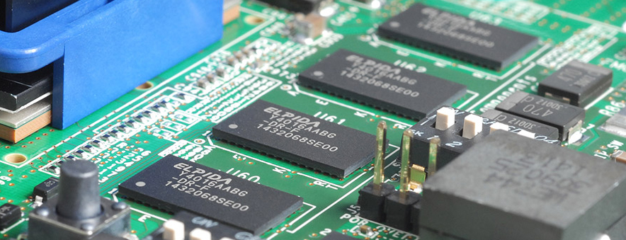
As DDR4 memory becomes more available and starts to make appearances in more products, one question we are frequently asked is: can I run JTAG tests on DDR4? The simple answer is – yes.
DDR4 is the next variation of dynamic RAM operating at higher speeds and lower voltages. It is not interchangeable with earlier DDR2 and DDR3 DRAM. The lower operating voltages of DDR4, 1.2V compared to 1.5V for DDR3, offers a useful power reduction. DDR4 also offer higher data transfer speeds ranging from 1600 to 3200 Mb/s compared to DDR3 which runs between 800 and 2133 Mb/s.
JTAG testing of memory
When we test using JTAG we are looking to see that the PCB has been correctly assembled. The tests will check that the correct parts have been used, that they are operational and, most importantly, whether there are any short-circuit or open-circuit faults on the board. When we perform tests with DRAM we use the JTAG boundary-scan enabled devices on the board to exercise the address and data busses to write values to memory and then read them back. Using carefully selected sequences of test patterns we can not only detect that a fault exists but diagnose the location of the fault.
We have shown that DDR4 memory can be tested in a similar way to other SDRAM types. However, DDR4 does offer some additional features over DDR3; in many implementations it has a test enable pin (TEN). Smaller devices may not have this as it is only compulsory on larger devices. The TEN pin puts the device into a “connectivity test mode” that makes it easier and quicker to verify that the device is correctly mounted on the board with no opens or shorts.
DDR4 Memory Modules (DIMMs) do not have the TEN pin on the connection to the mother board and so must be tested in a similar way to earlier memory types. However, if you are designing a board with DDR4 mounted directly on the PCB we recommend that you wire the TEN pin to either a JTAG enabled I/O pin or to a test header so the device can be put into connectivity test mode.
What does the connectivity test mode do?
When placed in Connectivity Test (CT) mode the device pins are divided into an input set and an output set. Between these pins are a set of asynchronous logic gates, defined in the JEDEC® DDR4 specification. By sending different signals to the input pins and checking the output pins we can quickly establish if there are any shorts or opens. CT mode is designed specifically to work with boundary-scan devices allowing test patterns to be entered on the test input pins in parallel and read from the outputs in parallel. This is quicker than writing and reading patterns to the memory.
Other DDR types
LPDDR4 – Low Power DDR does not have a TEN pin and must be tested the same way as DDR3 and earlier types.
GDDR5 – Graphics DDR – is not, as the name might suggest, a successor to DDR4; it actually predates it. GDDR5 does however have a test mode which enables the pins to be driven in parallel then the received values read back serially. This enables connectivity to be tested relatively simply. This is a form of boundary-scan, but should not be confused with 1149.1/JTAG.
Conclusion
In summary, DDR4 memory can be quickly and reliably tested using JTAG, either by using the same process used in DDR3 (memory write/reads to test connectivity) or using the TEN pin to place the device into connectivity test mode. Devices offering access to the TEN pin will enable faster testing than with previous types of SDRAM.
XJTAG will be adding DDR4 parts to its XJEase library soon for all customers in maintenance. If you have an urgent need of DDR4 memory tests, please contact us.
Other resources
What is JTAG?
And how can I make use of it?
High-Level Guide to JTAG
See what JTAG can do
Technical Guide to JTAG
A low-level look at how JTAG is implemented


