Introduction
The IEEE1149.1 (JTAG) standard does not explicitly support the testing of analogue devices, but it is easily possible to test in-circuit analogue functions using XJTAG. This application note describes a real-world example of testing an analogue RGB video port, as a demonstration of the type of solution that can be used. This type of solution can be easily adapted to test a variety of analogue functions.
The Circuit to be Tested
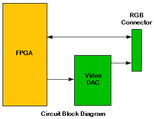
The circuit discussed in this application note contains a JTAG-compliant Xilinx FPGA driving an Analog Devices video DAC that, in turn, drives an external RGB port. A production requirement is to test the video DAC function and the integrity of the RGB connector. The following block diagram shows the relationship of the relevant circuit elements, and an extract from the board circuit diagram can be viewed here.

The 10-bit video DAC is an Analog Devices ADV7193 and its datasheet is available here. In order to test this device, a method of generating and measuring analogue voltages at the RGB connector is required. Analogue RGB values for the Red, Blue and Green signals (refer to the circuit diagram) can be generated by applying the appropriate digital signal levels to the DAC inputs, but how do we measure these analogue values? The solution is to create an RGB ‘test’ connector, which can be plugged into the board being tested. The connector contains a small serial ADC that can be controlled using the ‘digital’ signals to and from the FPGA, which are available at the connector.
The ADC must have more bits of resolution than the DAC, so that the least significant bits of the DAC can be tested reliably. A Maxim MAX1246 ADC was chosen due to its low cost, small size and ready availability. This provides 12 bits of measurement resolution against 10 bits of DAC resolution, just enough for our purposes. The circuit for the add-on test connector is shown here, and a datasheet for the MAX1246 is available here.
From the main circuit diagram it can be seen that there are four ‘digital’ signals available at the RGB connector (Vsync,Hsync, SDA and SCL) and that these are connected to FPGA I/O ports. The MAX1246 requires a 3-wire SPI serial interface that will use three of these connections, and the fourth can be used to provide power to the test connector. Although the power supply is drawn through a 120Ω resistor on the circuit under test, the low power consumption of the ADC (2mA maximum) ensures that the voltage drop across this resistor is limited to 0.25V and therefore that the power supply to the Maxim ADC is within allowable limits (between 2.7V and 3.6V).
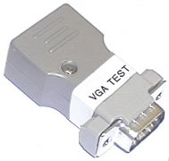
The ADC circuit is assembled on a small prototyping board and mounted into the housing of a suitable connector, providing a very neat test solution, as shown in this photograph:

XJEase programming for the test connector
Having designed a test solution, it is now an easy task to write an XJEase device file to generate analogue voltages at the connector and check them using the ADC. The complete code for this test program can be downloaded here.
The device file preamble is standard and defines the ADC7123 pin names, but it should be noted that the signals available at the RGB connector which are not available on the DAC have to be referenced with respect to the connector name (in this case CN20). This is done in XJEase using the pin number syntax DEVICE_NAME:PIN_NUMBER.
These are the only lines of code which would require modification if this DAC device is used on another board. TheDISABLE DEVICE statement ensures that power is always supplied to the test connector during connection testing, which prevents any other pin of the ADC being driven higher than its Vcc.
DEVICE NAME := "Video DAC ADV7123"

  PINS
    RED    := 48, 47, 46, 45, 44, 43, 42, 41, 40, 39;
    GREEN  := 10, 9, 8, 7, 6, 5, 4, 3, 2, 1;
    BLUE   := 23, 22, 21, 20, 19, 18, 17, 16, 15, 14;
    nBLANK := 11;
    nSYNC  := 12;
    CLK    := 24;
    SDOUT  := CN20:15;
    SDIN   := CN20:12;
    VCC    := CN20:13;
    SCLK   := CN20:14;
  END;

  DISABLE DEVICE
    // Power must be applied to ADC at all times to avoid
    // any input being driven above the power rail.
    VCC  := 1;
  END;

  TEST COVERAGE
    SDOUT  := WRITE;
    SDIN   := READ;
    SCLK   := WRITE;
    VCC    := WRITE;
    RED    := WRITE;
    GREEN  := WRITE;
    BLUE   := WRITE;
    nBLANK := WRITE;
    nSYNC  := WRITE;
  END;
END;
The next section defines various constants used in the file which make the code more readable and maintainable. TheDEBUG variable can be set non-zero to provide additional debugging output during code execution.
// ADC channel assignment
INT RED_CHANNEL       := 0;
INT GREEN_CHANNEL     := 1;
INT BLUE_CHANNEL      := 2;
INT SPARE_CHANNEL     := 3;

// Set for additional debug output
INT DEBUG             := 0;

//------------------------------------------------------
// ADC Parameters
//------------------------------------------------------

INT ADC_VREF_MV       := 2048;
INT ADC_NUM_BITS      := 12;

//------------------------------------------------------
// DAC Parameters
//------------------------------------------------------

INT DAC_NUM_BITS      := 10;
INT DAC_FULLSCALE_MV  := 1400; // DAC Red/Blue output voltage (mV) at full scale
INT DAC_SYNCOFFSET_MV := 600;  // DAC Green output voltage blank level offset
The ADC communicates with the system using a 3-wire serial (SPI or Microwire compatible) bus. Commands are issued to the ADC by setting up a bit on the Data Input (DIN) pin and generating a rising edge on the Clock (SCLK) pin. Data is read from the ADC by generating a falling edge on the SCLK pin and sampling the data in the Data Output (DOUT) pin.
The SPI bus is driven from XJEase using two small interface routines, SPI_WriteSerial and SPI_ReadSerial. The routines can handle any length of serial transfer (although this application only requires 8-bit transfers) and so can be easily reused in other applications. SPI_WriteSerial shifts out a number of bits, most-significant bit first, and toggles the clock for each bit.
SPI_WriteSerial( INT value )()
  INT i;
  FOR i := 0 FOR 8
    SET SCLK := 0, SDIN := value[7 - i];
    SET SCLK := 1;
  END;
  SET SCLK :=0;
END;
The SPI_ReadSerial routine performs the opposite function and assembles data by toggling the clock and shifting in the read data. Again, this can be performed for any specified number of bits. The code for these routines can be cut and pasted into any device file which requires an SPI interface.
SPI_ReadSerial()( INT value )
  INT bit, i;
  value := 0;

  SET SDIN := 0, SCLK := 1;

  FOR i := 0 FOR 16
    SET SCLK := 0;
    SET SCLK := 1,bit := SDOUT;
    value := (value << 1) | bit;
  END;
  SET SCLK := 0;
END;
The ADC_Read routine reads a value from one of the four ADC channels and returns a 12-bit result. The command written to the ADC is comprised of a start bit (bit 7) to define the beginning of a control byte, a channel select field (bits 6..4), a unipolar/bipolar flag (bit 3), a single-ended/differential flag Bit 2) and clock/power selection options (bits 1..0). In this application, the ADC is always in internal clock mode. The command byte is assembled according to the required channel, and a data read is then performed to read back the converted analogue value for the required channel. The value is checked for validity (bits 3..0 should always be zero) and returned to the calling routine.
ADC_Read(INT channel WIDTH 2)(INT result WIDTH 12)

  INT value WIDTH 16;
  INT sel WIDTH 3;
  INT command WIDTH 8;

  IF (channel=0) THEN sel := 1; END;
  IF (channel=1) THEN sel := 5; END;
  IF (channel=2) THEN sel := 2; END;
  IF (channel=3) THEN sel := 6; END;

  // Unipolar, single-ended, internal clock mode, selected channel.
  command := 1[0] : sel[2..0] : 0x0e[3..0];
  SPI_WriteSerial(command);
  SPI_ReadSerial()(value);

  // Value is held in top 12 bits.
  result := value[15..4];

  IF (value[3..0] != 0) THEN
    PRINT("\nVGA Test cable response error - is the cable connected?\n");
    EXIT;
  END;

  IF DEBUG THEN PRINT("ADC value for channel ", channel,
                      " is 0x", HEX(result), "\n"); END;

END;
The Test_Channel routine checks an individual ADC channel by checking sync and blanking levels and then confirming that setting each bit at the DAC input generates an increasing analogue voltage. The routine can be called for each of the active analogue channels (Red, Blue and Green).
For each test, a digital data value is set up on the DAC inputs and the converted analogue value is read back from the ADC using the ADC_Read routine described above. This process is repeated for each of the 10 DAC bits in turn and a check is made to ensure that the analogue value increases as expected. A final check is made with all bits set, to ensure that the maximum value is read back. As sync is encoded on the Green channel, an additional check is made on the green channel to ensure that the value during blanking is greater than the value during sync.
Test_Channel(INT channel WIDTH 2)(INT result)

  INT adc_value WIDTH 12;
  INT bit;
  INT dac_value WIDTH 10;
  INT last_adc_value WIDTH 12;
  INT timeout;

  IF DEBUG THEN PRINT("Testing channel ", channel, "...\n"); END;
  result := 1;

  // Check for a valid channel requested.
  IF ((channel > BLUE_CHANNEL) || (channel < RED_CHANNEL)) THEN
    PRINT("Invalid ADC channel ", channel, " requested.\n");
    RETURN;
  END;

  // Check channel value during blanking and, for the green channel,
  // confirm that the blanking level is above the sync level.
  SET nSYNC := 1, nBLANK := 0, RED := 0x3ff, GREEN := 0x3ff, BLUE := 0x3ff, CLK := 0;
  SET CLK := 1;
  FLUSH;
  timeout := NOW+100;
  DO WHILE NOW < timeout END;
  ADC_Read(channel)(adc_value);

  IF (channel=GREEN_CHANNEL) THEN
    IF (adc_value < 0x400) THEN
      PRINT("ERROR - Green  Blanking level wrong.\n");
      RETURN;
    END;
  ELSE
    IF (adc_value > 1) THEN
      PRINT("ERROR during BLANKING.\n");
      RETURN;
    END;
  END;

  // Check channel value during sync.
  SET nSYNC := 0, nBLANK := 0, RED := 0x3ff, GREEN := 0x3ff, BLUE := 0x3ff, CLK := 0;
  SET CLK := 1;

  ADC_Read(channel)(adc_value);

  IF (adc_value > 1) THEN
     PRINT("ERROR during SYNC.\n");
     RETURN;
  END;

  last_adc_value := adc_value;

  // De-activate blank and sync inputs.
  SET  nSYNC:= 0, nBLANK := 1;

  // Check channel value for each DAC digital bit [9..0].
  FOR bit := 0 FOR 11

    IF (bit = 10) THEN
      dac_value := 0b1111111111;
    ELSE
      dac_value := (1<<bit); // single bit set
    END;

    IF channel = RED_CHANNEL   THEN
      SET RED := dac_value, GREEN := 0,         BLUE := 0,         CLK := 0;
    END;
    IF channel = GREEN_CHANNEL THEN
      SET RED := 0,         GREEN := dac_value, BLUE := 0,         CLK := 0;
    END;
    IF channel = BLUE_CHANNEL  THEN
      SET RED := 0,         GREEN := 0,         BLUE := dac_value, CLK := 0;
    END;

    // Rising edge on clock to latch RGB values in video DAC.
    SET CLK := 1;

    // Read the required colour channel value.
    ADC_Read(channel)(adc_value);
    IF DEBUG THEN
      PRINT("Bit ", bit, " DAC value set = ", dac_value,
            " ADC value:",adc_value," Test value:",last_adc_value,"\n");
    ELSE
      PRINT(".");
    END;

    // Check that the value has increased on every bit.
    IF (adc_value < last_adc_value) THEN
      PRINT("ERROR on channel ", channel, " bit ", bit, "\n");
      IF (!DEBUG) THEN RETURN; END;
    END;

    // Value for next bit should be at least 1.9 times this.
    // 1.9 ~= 121/64
    last_adc_value := (adc_value*121) >> 6;

  END;

  IF DEBUG THEN PRINT("Channel ", channel, " tested OK.\n"); END;

  result := 0;
  RETURN;

END;
Additional Applications
This type of analogue measurement can readily be transferred to other applications, such as the circuit for an analogue video test connector for a digital video connector available here.
Summary
This example demonstrates the ease with which XJTAG can be adapted to perform complex testing of analogue ports in system.
All of the files mentioned in this application note can be downloaded as a single ZIP file.

