XJTAG delivers time and cost savings to PartnerTech
PartnerTech, one of Europe’s largest business-to-business EMS companies, needed a sophisticated boundary scan solution to improve diagnosis times and test coverage on densely-packed circuit boards, and which would eradicate the need to build dedicated in-circuit test (ICT) fixtures and thereby reduce non-recurring engineering (NRE) expenses.
Customers of electronics manufacturing services (EMS) providers are putting pressure on lead times to secure the first-to-market benefits that define success for high-tech developers. This is forcing EMS companies to find time savings throughout all the activities involved in manufacturing new products. A significant proportion of this time is the development and implementation of a suitable test strategy, so savings here can dramatically reduce time to market for new products. At the same time, the challenges associated with testing modern boards are intensifying, as physical access is now severely restricted, and board complexity is skyrocketing in order to increase functional capability while observing the many limitations on board sizes.
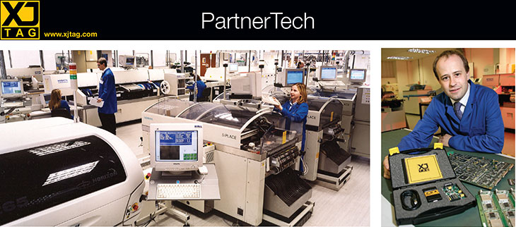
To overcome these challenges, PartnerTech selected XJTAG as its boundary scan test solution partner and has implemented the XJTAG system at its UK manufacturing facilities at King’s Lynn and Cambridge. The XJTAG system integrates seamlessly with PartnerTech’s in-circuit and functional test fixtures. PartnerTech provides customers – primarily in telecommunications, IT, the engineering industry and medical technology sector – with a wide range of product lifecycle services from design, design prototyping and new product introduction, to production, logistics, distribution and after sales.
According to PartnerTech, for many board types, the XJTAG system eradicates the need to build a dedicated in-circuit test (ICT) fixture and this has enabled it to reduce non-recurring engineering (NRE) expenses by up to £10k per printed circuit board type. PartnerTech manufactures a significant number of diverse products each month of which around half can utilise XJTAG, either exclusively or in conjunction with functional, ICT or flying probe testing. These boards are typically high complexity, densely populated circuits with at least one JTAG device.
“We looked at other competitive boundary scan test products, and some were as much as twice the cost, but found that XJTAG with its versatility, reusability of scripts and a high level of diagnostics made it the most cost-effective solution”, said Tim Murrell, senior electronics engineer at PartnerTech.
“We are also finding that offering a sophisticated boundary scan solution such as XJTAG gives us a competitive advantage in the market. Our OEM (original equipment manufacturer) customers are becoming more JTAG-aware and have been impressed that XJTAG can be used at the design and prototyping stage and right through into production, field support and repair – several customers already have their own XJTAG licence.”
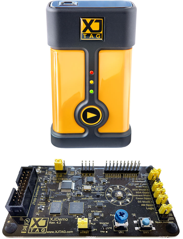
The powerful and easy-to-use XJTAG boundary scan system meets the growing market need for a cost-effective solution for testing complex printed circuit boards populated with ball grid array (BGA) and chip scale devices, which cannot be tested by traditional methods. The XJTAG system is designed to cut the cost and shorten the development cycle of electronic products and provides a unique solution that can test JTAG as well as non-JTAG devices. XJTAG can test a high proportion of a circuit including BGA and chip scale devices, SDRAMs, Ethernet controllers, video interfaces, flash memories, FPGAs, microprocessors and many other devices. XJTAG can test a high proportion of a circuit including BGA and chip scale devices, SDRAMs, Ethernet controllers, video interfaces, flash memories, FPGAs, microprocessors and many other devices. XJTAG can be used to debug and test any circuit provided it has at least one JTAG-compliant device present.

XJTAG represents the biggest single step in test diagnostics that I have seen in years.
It is an extremely versatile and flexible boundary scan solution, which, unlike some JTAG test products, integrates seamlessly with other test equipment. Not only will it help to reduce our test NRE expenses but it will enable us to significantly improve our diagnosis times and test coverage on densely packed circuit boards which are increasingly populated with flip chips, ball grid array and chip scale devices.

Company: PartnerTech
Nature of business: Electronics Manufacturing Services (EMS) provider
Customers: OEMs in telecommunications, IT, the engineering industry and medical technology sector
Locations: Sweden, Norway, Finland, Poland, UK, United States and China
Employees: Approx. 2,000
Revenues: SEK 3 billion (£226 million)
Web site: www.partnertech.co.uk

Configure your products


