XJFlash is an FPGA-based advanced and innovative method that uses JTAG for high-speed in-system programming (ISP) of flash memories – all serial and parallel flash devices are supported. The most common use of XJFlash is programming the SPI/QSPI NOR flash used to configure an FPGA.
With XJFlash you can use the FPGA on your board to achieve flash programming speeds up to 50 times faster than those possible using conventional boundary scan techniques, often reaching the maximum speed for the flash memory.
Custom Solutions – Automatically Generated
XJFlash allows you to automatically generate customised programming solutions for the flash memory devices connected to FPGAs and FPGA SoCs (such as Xilinx Zynq® and Intel Cyclone® V) on your board.
The functional capabilities of the FPGA are harnessed to provide the fastest possible programming speeds. XJFlash automatically generates a custom design for each FPGA/flash combination, allowing you to achieve the best programming times, whilst not requiring you to do any FPGA development.*
If your flash memory is connected to an FPGA from Intel (Altera), Xilinx, Microsemi or Lattice, XJFlash uses the FPGA’s standard JTAG port to offer an in-circuit programming alternative to a SPI programmer or parallel flash programmer. XJFlash support all SPI modes (single-bit, dual, quad, QSPI, and octal) as well as parallel NOR flash devices.
*A licensed version of the relevant FPGA manufacturer’s tools will be required during the configuration of XJFlash. Free versions are sufficient for many devices.
Test Integration
XJFlash programming can be easily integrated into your XJTAG test system using XJDeveloper. All XJFlash programming can be run as part of an XJRunner boundary scan test project.
Configurable Flash Programming
It doesn’t matter whether you need to program a single flash memory device, or multiple devices that are connected in series, to expand the address space, or in parallel, to make a wider data bus, you can use XJFlash to speed up your programming operations.
Custom development
XJFlash can also be used for standalone programming requirements including direct access to I²C and SPI busses or custom protocols such as Microchips ICSP.
The required connections do not need to come from an FPGA on the target board. Providing the protocol signals are available on a header on that board, it should be possible to use XJFlash to achieve fast programming as part of an XJTAG solution.
XJFlash Example Timings
Minimum theoretical time for conventional boundary scan: 35 minutes.
Total XJFlash run time: 10.5 s to 32.6 s.
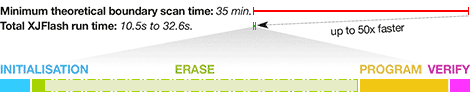
XJFlash will automatically step through four stages each time a flash device is programmed:
Initialisation – The FPGA connected to the flash is configured with the XJFlash image required for the target board. Example time: 2.1 s.
Erase – The flash can be erased using one of two algorithms. The basic erase will simply erase all blocks within a defined range (this may be the whole flash or just the space needed for the image to be programmed). The more intelligent erase will use the fact that it is quicker to read the flash than to erase it; as such it reads from each address and only starts erasing if some data is found. This step can be skipped if it is known that the flash will always be blank before it is programmed.
Example time – intelligent erase enabled: 0.9 s with a device already erased, to 23 s with a fully programmed device (limited by erase time of device).
Program – Data from the target images is streamed into the FPGA through its JTAG port. The FPGA then programs this data into the connected flash(s). Multiple files can be specified and programmed at defined offsets. This step can be bypassed if only verification is required.
Example time: 6.2 s (limited by the programming speed of the device).
Verify – The verification checks every byte in the flash against the specified file(s), ensuring there are no data bit errors. This step can be bypassed if only programming or erasing is required.
Example time: 1.8 s with TCK at 10 MHz, reducing to 1.3 s with TCK at 20 MHz.
These example times are provided for a Spartan-6 XC6SLX9 programming a 2 MByte pseudorandom data file into the FPGA’s SPI configuration PROM.
Example Timings Using a Xilinx Zynq®-7000 series SoC
A 256 Mbit file can be programmed into a SPI NOR flash and verified in around 46 s, depending on the TCK speed and the memory type being used*; 32 Mbit of code takes just over 7 s.
Adding an initial erase cycle adds only 3.1 s for an empty 256 Mbit flash, or 54 s for a full one. That drops to 0.4 s and between 6.5 and 9.2 s respectively for a 32 Mbit device.
* TCK = 66 MHz, pseudorandom data file. Time varies with flash type.
Example Timings Using a Xilinx Zynq® UltraScale+™ series SoC
A 256 Mbit file can be programmed into a SPI NOR flash and verified in around 42 s, depending on the TCK speed and the memory type being used**; 32 Mbit of code takes 7 s.
Adding an initial erase cycle adds only 2 s for an empty 256 Mbit flash, or 57 s for a full one. That drops to 0.3 s and 6.9 s respectively for a 32 Mbit device.
** TCK = 30 MHz, pseudorandom data file. Time varies with flash type.
Can I use XJFlash?
In order to use XJFlash all of the data, address and control signals on the flash device(s) must be connected to an FPGA on the target board. This can be a configuration PROM, or a flash device connected to any general purpose I/O pin. These connections can be direct, indirect, dedicated or shared:
Direct connections – YES


The flash is directly connected to the FPGA.
Indirect connections – YES

- The flash is connected to the FPGA via a buffer
- Some of the address signals are shared with the data signals and connected via a latch.
- There is another configurable device, such as a CPLD between the flash and the FPGA.
Shared connections – YES

The flash is connected to the FPGA in one of the modes described above but these connections are shared with another device (such as a processor).
No connections – YES (with design changes)

If your design contains an FPGA but the flash is not connected in any of the configurations described, it may be possible to use spare pins on the FPGA to establish connections to the flash. These connections would not be used in the mission mode of the board but would allow you to use XJFlash to perform fast flash programming. If your FPGA is already connected to the same address/data bus as the flash then this may not require many extra signals.
No FPGA – Not directly

Unfortunately, it is not possible to use XJFlash if there is no FPGA. However, if it is possible to bring the connections of the flash to a header or test points on the board, XJFlash fast programming can be used via those connections using an XJAccelerator card.
Alternatively, it may be possible to do fast flash programming using the debug interface on a processor – please contact us to see if you can use this approach on your board.
Compatibility
- Intel (Altera) – Arria GX, Arria II GX, Arria II GZ, Arria V, Arria V GZ, Arria 10, Cyclone, Cyclone II, Cyclone III, Cyclone III LS, Cyclone IV E, Cyclone IV GX, Cyclone V, Stratix, Stratix GX, Stratix II, Stratix II GX, Stratix III, Stratix IV, Stratix V, Stratix 10
- Lattice – MachXO2, LatticeECP3, LatticeXP2
- Microsemi – IGLOO2, ProASIC3, ProASIC3E, ProASIC3L, SmartFusion2
- Xilinx – Artix-7, Kintex-7, Kintex UltraScale, Kintex UltraScale+, Spartan-3, Spartan-3A, Spartan-3E, Spartan-6, Spartan-7, Virtex-II, Virtex-II Pro, Virtex-4, Virtex-5, Virtex-6, Virtex-7, Virtex UltraScale, Virtex UltraScale+, Zynq-7000, Zynq UltraScale+
This list is continuously growing, so contact us for the latest details.
All trademarks are the property of their respective owners.
Recommended system requirements
- Intel® Core i3, i5, i7 processor or equivalent (any generation)
- Microsoft® Windows® 8, Windows 8.1, Windows 10 (1607 and later), or Windows 11 (32 or 64 bit)
- 4 GB of RAM
Frequently asked questions
General
How can XJFlash be 50 times faster than programming with conventional boundary scan?
With conventional boundary scan each signal change requires one complete test vector to be scanned through the JTAG chain. XJFlash configures the FPGA with a programming algorithm so it can change these signals at its operating clock speed. JTAG is still used to stream the data to be programmed into the FPGA but the control of the signals on the board is done by the FPGA.
I use a fast flash programmer already, why should I consider using XJFlash?
XJFlash makes use of the FPGA resources already designed into the board. This means it is possible to use a single JTAG tool to boundary scan test the board and program it in one step, making it faster than swapping between tools on the production line. Furthermore, using in-system programming removes the need to pre-program flash devices, allowing the latest flash image to always be used and allowing the same tools to be used during development, production, and repair.
Technical questions
What flash devices are supported?
XJFlash has built-in support for a wide range of parallel and serial NOR flash devices. Support for NAND devices is also available.
What FPGAs are supported?
XJFlash can be used on a wide range of FPGAs from Intel (formerly Altera), Lattice, Microsemi (formerly Actel), and Xilinx.
What Xilinx Zynq SoCs are supported?
XJFlash provides NOR flash programming of memories connected to Xilinx Zynq-7000 and Zynq-UltraScale+ SoCs. This includes the following families: Xilinx XC7Z007S, XC7Z010, XC7Z012S, XC7Z014S, XC7Z015, XC7Z020, XC7Z030, XC7Z-35, XC7Z045, XC7Z100, XCZU2, XCZU3, XCZU4, XCZU5, XCZU6, XCZU7, XCZU9, XCZU11, XCZU15, XCZU17, XCZU17, XCZU19. New parts are always being added, so please contact us if your device isn’t listed.
What if I want to program a type of device that's not listed?
The range of devices programmable using XJFlash is continuing to grow, so if you want to program a device that is not currently listed then let us know.
Can I use XJFlash on boards I’ve already designed?
Yes. XJFlash transfers all data from the PC to the board via the FPGA’s JTAG port, which is commonly brought to a header on the board for use during development. Therefore, provided this has been done and the flash to be programmed is accessible from the FPGA, XJFlash can be used.
My flash is not connected directly to the FPGA on my board, might I still be able to use XJFlash?
Yes. XJFlash can easily be customised to support scenarios where the FPGA is not directly connected to the flash to be programmed. For example, the signals could go through buffers, latches, a CPLD or other forms of logic, and XJFlash can still be used. Furthermore, even if some of the signals have to be serialised to get them between the FPGA and a CPLD, XJFlash can be used.
Not all the signals on my flash are accessible from the FPGA, surely that makes it impossible to use XJFlash?
This all depends on the type of flash to be programmed and which signals are accessible. XJFlash is designed to allow the FPGA to be included in a JTAG chain with other devices, which means some signals can be controlled using boundary scan from other devices whilst XJFlash runs on the FPGA. Contact us to find out if XJFlash can work in your case.
Is this limited to only programming FPGA configuration devices?
No. Due to XJFlash’s ability to create custom FPGA images for each board design, it is not restricted to only programming the configuration device.
I’m not an FPGA developer, will this be too complicated for me?
No. Although XJFlash requires a custom FPGA image for each design of board, this is an automated process controlled by XJFlash. This requires the relevant FPGA vendor’s tools to be installed on the PC used to develop the tests, but you won’t have to use them yourself.
Will I have to buy extra FPGA tools to be able to use XJFlash?
This depends on the FPGA being used. Many FPGAs are supported by free versions of the various vendors’ own tools. For these FPGAs no additional products would need to be purchased. For larger FPGAs, contact your FPGA developers, or contact us.
Can I simultaneously program multiple PCBs, each with their own flash devices?
Yes – because XJFlash can be added to a sequence of production tests, concurrent programming can be implemented in exactly the same way as concurrent boundary scan testing.
Can I use XJFlash both in high-volume and low-volume/high-mix production situations?
Yes – because XJFlash can be incorporated in your production tests and it uses the FPGA built on to the board, there are very few time overheads and no hardware modifications required when switching between different board designs.
This can’t be faster than the FPGA vendor’s programming tool, can it?
XJFlash has been found to be faster than many commonly used flash programming tools, so why not try it and see for yourself? Contact us.
Do you support fast Flash programming attached to microprocessors, CPUs, DSPs?
Yes – please contact us for more details.
What are the recommended system requirements to run XJFlash?
- Intel® Core i3, i5, i7 processor or equivalent (any generation)
- Microsoft® Windows® 8, Windows 8.1, Windows 10 1607 and later, Windows 11 (32 or 64 bit)
- 4 GB of RAM
Free evaluation / Licensing
What are the differences between the trial version and the purchased product?
There is no difference between the functionality of the purchased product and the free evaluation version. We provide full technical support by telephone and email, to help with the set-up or troubleshoot any issues during your trial. You will also have access to XJTAG’s device test libraries and latest software upgrades, during your 30-day evaluation period.
Can I convert my trial version to a purchased product?
Yes. If you already have XJFlash for evaluation, you can continue using it without interruption by purchasing the full licence. Contact your XJTAG distributor to make a purchase and have your licence extended.
Do I need to purchase an XJFlash licence for each XJRunner I want to use?
No. An XJFlash licence is required to create the programming configuration for a particular board, after which that configuration can be used with any XJRunner on the same board.
What clients say…
![]()
For a 128 Mbit device, XJFlash can reduce the total programming time to less than 20 seconds, with an average write-cycle time of under 2 µs.
Jeff Bader, Senior Director of Marketing, Micron Technology
![]()
We achieved tremendously valuable time savings, cutting the time to program large FPGAs from several minutes to just 35 seconds.
Chris Beynon, CTO, Active Silicon

- High-speed flash programming
- Fast firmware upgrade
Key benefits
- Cuts flash programming times
- SPI, QSPI, parallel NOR flash devices supported
- Support for NAND flash devices available on request
- Shortens development cycles
- No need for additional equipment
- Can be used for fast firmware upgrade
- No FPGA development required
Flexible Licensing Options
- Hardware licence
– held in the JTAG controller so you can use XJTAG on any number of PCs - Network licence
– held on a networked license server available from anywhere in the world